(Hong Kong)

Product Summary
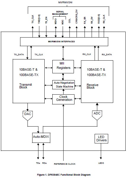
The DP83848CVV+ is a Transceiver fully featured 10/100 single port Physical Layer device offering low power consumption, including several intelligent power down states. These low power modes increase overall product reliability due to decreased power dissipation. Supporting multiple intelligent power modes allows the application to use the absolute minimum amount of power needed for operation. The DP83848CVV+ includes a 25MHz clock out. This means that the application can be designed with a minimum of external parts, which in turn results in the lowest possible total cost of the solution. The applications of the DP83848CVV+ are: High End Peripheral Devices, Industrial Controls and Factory Automation, General Embedded Applications3848CVV+.
Parametrics
DP83848CVV+ absolute maximum ratings: (1)Supply Voltage (VCC): -0.5 V to 4.2 V; (2)DC Input Voltage (VIN): -0.5V to VCC + 0.5V; (3)DC Output Voltage (VOUT): -0.5V to VCC + 0.5V; (4)Storage Temperature (TSTG): -65oC to 150℃; (5)Max case temp for TA = 70℃: 92 ℃; (6)Max. die temperature (Tj): 150 ℃; (7)Lead Temp. (TL)(Soldering, 10 sec.): 260 ℃; (8)ESD Rating(RZAP = 1.5k, CZAP = 100 pF): 4.0 kV.
Features
DP83848CVV+ features: (1)Low-power 3.3V, 0.18μm CMOS technology; (2)Low power consumption < 270mW Typical; (3)3.3V MAC Interface; (4)Auto-MDIX for 10/100 Mb/s; (5)Energy Detection Mode; (6)25 MHz clock out; (7)SNI Interface (configurable); (8)RMII Rev. 1.2 Interface (configurable); (9)MII Serial Management Interface (MDC and MDIO); (10)IEEE 802.3u MII; (11)IEEE 802.3u Auto-Negotiation and Parallel Detection; (12)IEEE 802.3u ENDEC, 10BASE-T transceivers and filters; (13)IEEE 802.3u PCS, 100BASE-TX transceivers and filters; (14)Integrated ANSI X3.263 compliant TP-PMD physical sublayer with adaptive equalization and Baseline Wander compensation; (15)Error-free Operation up to 137 meters; (16)Programmable LED support Link, 10 /100 Mb/s Mode, Activity, and Collision Detect; (17)Single register access for complete PHY status; (18)10/100 Mb/s packet BIST (Built in Self Test); (19)48-pin LQFP package (7mm) x (7mm).
Diagrams
 |
 DP83016AUG |
Other |
|
Data Sheet |
Negotiable |
|
||||
|
DP8308 |
Other |
|
Data Sheet |
Negotiable |
|
||||
|
DP8310 |
Other |
|
Data Sheet |
Negotiable |
|
||||
|
DP8311 |
Other |
|
Data Sheet |
Negotiable |
|
||||
|
DP83223 |
Other |
|
Data Sheet |
Negotiable |
|
||||
 |
DP83223V |
|
IC NETWORK TRANSCEIVER 28-PLCC |
Data Sheet |
Negotiable |
|
||||